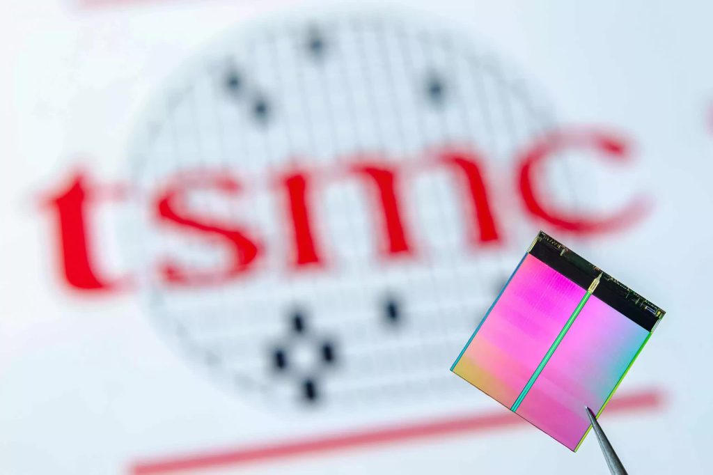
In short: TSMC has introduced that its A14 (1.4nm-class) chip manufacturing course of will enter manufacturing in 2028, following the rollout of its 2nm expertise later this 12 months and constructing on its present lineup of 3nm-class chips. The corporate says the A14 node represents a big leap in each efficiency and effectivity.
The roadmap was unveiled this week on the North American Know-how Symposium. As a part of the announcement, TSMC revealed plans for an middleman A16 node, slated for launch in late 2026. This node will function a stepping stone towards the extra transformative A14 course of.
A key spotlight of the A14 era is NanoFlex Professional, an enhanced transistor structure that allows chip designers to fine-tune configurations for optimum energy, efficiency, and space based mostly on the particular necessities of every software.

Whereas TSMC hasn’t disclosed all of the technical particulars of NanoFlex Professional, it is anticipated to construct on the corporate’s current FinFlex structure, which permits designers to mix completely different normal cell sorts – resembling high-performance, low-power, or area-efficient cells – inside a single block. NanoFlex Professional could supply even finer-grained management, doubtlessly on the transistor stage, or introduce smarter design instruments to speed up chip optimization.
In the meantime, manufacturing is already ramping up for TSMC’s third-generation 3nm-class course of, N3P, which formally entered mass manufacturing in This fall 2024. As an optical shrink of N3E, N3P is now powering high-performance chips for purchasers in each knowledge facilities and superior shopper expertise sectors.
Subsequent in line is N3X, anticipated to achieve quantity manufacturing within the second half of this 12 months. Tailor-made for max frequency, N3X delivers an extra 5 p.c efficiency achieve over N3P and helps voltages as much as 1.2V, an unusually excessive threshold for 3nm nodes. This makes it significantly well-suited for consumer CPUs and AI accelerators that prioritize uncooked velocity over energy effectivity.
TSMC Deputy COO Kevin Zhang famous that whereas smartphones as soon as led the best way in adopting new nodes, the AI increase has reversed that development. As we speak, AI chipmakers are the primary to embrace the newest and most superior course of applied sciences.
With N3P in full manufacturing, N3X on observe, and A14 on the horizon, TSMC is doubling down on its technique of providing a number of node enhancements to increase the lifecycle of its modern fabs and buyer IP. All of that is underpinned by an enormous $40 billion in capital expenditures for 2025, reinforcing the foundry’s place because the premier alternative for the world’s most superior semiconductors.